| Sign In | Join Free | My xxjcy.com |
|
| Sign In | Join Free | My xxjcy.com |
|
| Categories | High Density Interconnect PCB |
|---|---|
| Brand Name: | UAV PCB |
| Model Number: | As Per Customer's Model |
| Place Of Origin: | Dongguan China |
| Certification: | ISO 9001 / RoHS /UL / IATF 16949 (automotive) |
| MOQ: | Sample,1 Pc(5 Square Meters) |
| Price: | Based on Gerber Files |
| Packaging Details: | NA |
| Payment Terms: | ,T/T,Western Union |
| Supply Ability: | 100000㎡/Month |
| Place of Origin: | China |
| Delivery Time: | NA |
| PCB Type: | HDI Print Circuit Board |
| Material: | High Tg FR-4 |
| Impedance Control: | Yes |
| Copper Overall: | 0.5-5oz |
| Pcba: | Support |
| Quality Standard: | IPC Class 2 |
| Max.Board Size: | 528*600mm |
| Surface Finishing: | OSP/ENIG/ENEPIG |
| Quotation List: | Gerber Or BOM List |
| Thickness: | 1.6/1.2/1.0/0.8 or Custom |
| Layer Count: | 2/4/6/8/10 or Customized |
| Company Info. |
| Dongguan Xingqiang Circuit Board Technology Co., Ltd. |
| Verified Supplier |
| View Contact Details |
| Product List |
A Custom HDI White Oil Automotive PCB is a high‑performance automotive circuit board that combines HDI technology with a white solder mask. HDI enables high‑density interconnections, fine lines, and microvias, allowing miniaturization and reliable high‑speed signal transmission in limited spaces. The white solder mask provides excellent light reflection—critical for LED lighting applications—and enhances the visibility of silkscreen labels. Built to meet strict automotive standards, it withstands extreme temperatures, vibration, and humidity, making it ideal for automotive LED modules, sensors, and compact control systems requiring both performance and durability.
• HDI Technology: Utilizes microvias, blind/buried vias, and fine-pitch traces for
high component density and compact design.
• White Solder Mask: Features a white protective coating that offers superior light
reflection and high contrast for clear silkscreen printing.
• Automotive Grade: Manufactured with high TG materials and compliant with IATF 16949
standards, ensuring durability in harsh environments.
• Enhanced Reliability: Delivers stable electrical performance, excellent thermal
conductivity, and resistance to high temperatures, vibration, and
humidity.
1.Design and Engineering Preparation
The client provides design files (such as Gerber files), and the
engineering team conducts Design for Manufacturability (DFM)
analysis, optimizing the layout to ensure microvia and trace
accuracy, while selecting appropriate substrate materials (such as
FR-4 or high-frequency laminates).
2.Inner Layer Fabrication and Drilling
Fabricating inner-layer circuits on the substrate: Copper layers
are etched to form circuits via photolithography, followed by laser
drilling (or mechanical drilling) to create microvias (typically
with diameters less than 0.15mm) for high-density interconnections.
3.Pore metallization and lamination
Chemically plate the holes with copper or fill them with conductive
materials to make the hole walls conductive; then laminate all
inner and outer layers together under high temperature and pressure
to ensure precise alignment of each layer.
4.Outer Layer Manufacturing and Surface Treatment
Add outer layer circuit: After graphic transfer and etching,
perform surface treatment (such as gold immersion, OSP, or silver
immersion) to enhance solderability and oxidation resistance.
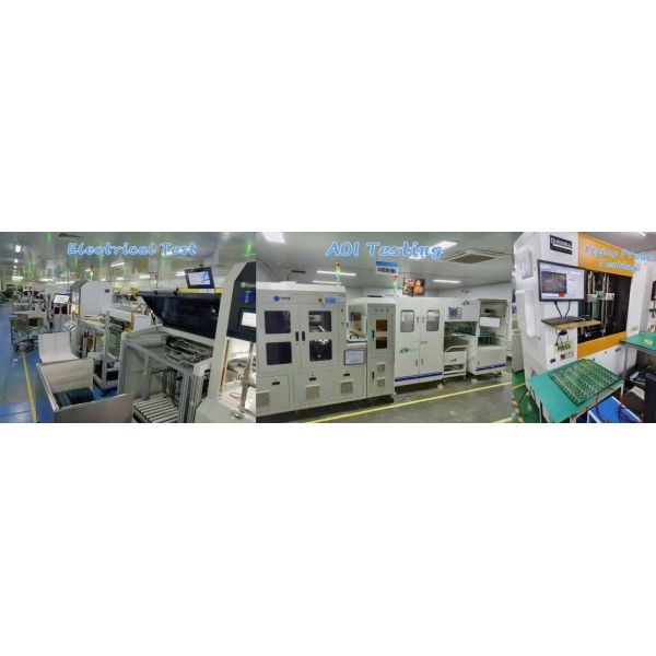
5.Testing and Final Processing
Conduct rigorous circuit function testing (including AOI and
electrical testing), confirm defect-free results, then proceed with
trimming, cleaning, and packaging for shipment.

Factory showcase

PCB Quality Testing
Certificates and Honors


|
